5 Band CW QRP Transceiver Direct Conversion Receiver Block
Part of the 5 band transceiver.
The direct conversion receiver block takes the antenna input (J1) from a transmit board’s LPF and outputs audio I/Q for feeding to the audio phasing and amplifier board. It
includes a front end switch to isolate the receiver during transmit, switchable attenuator and pre-amp, and a splitter to feed a signal to an external receiver.
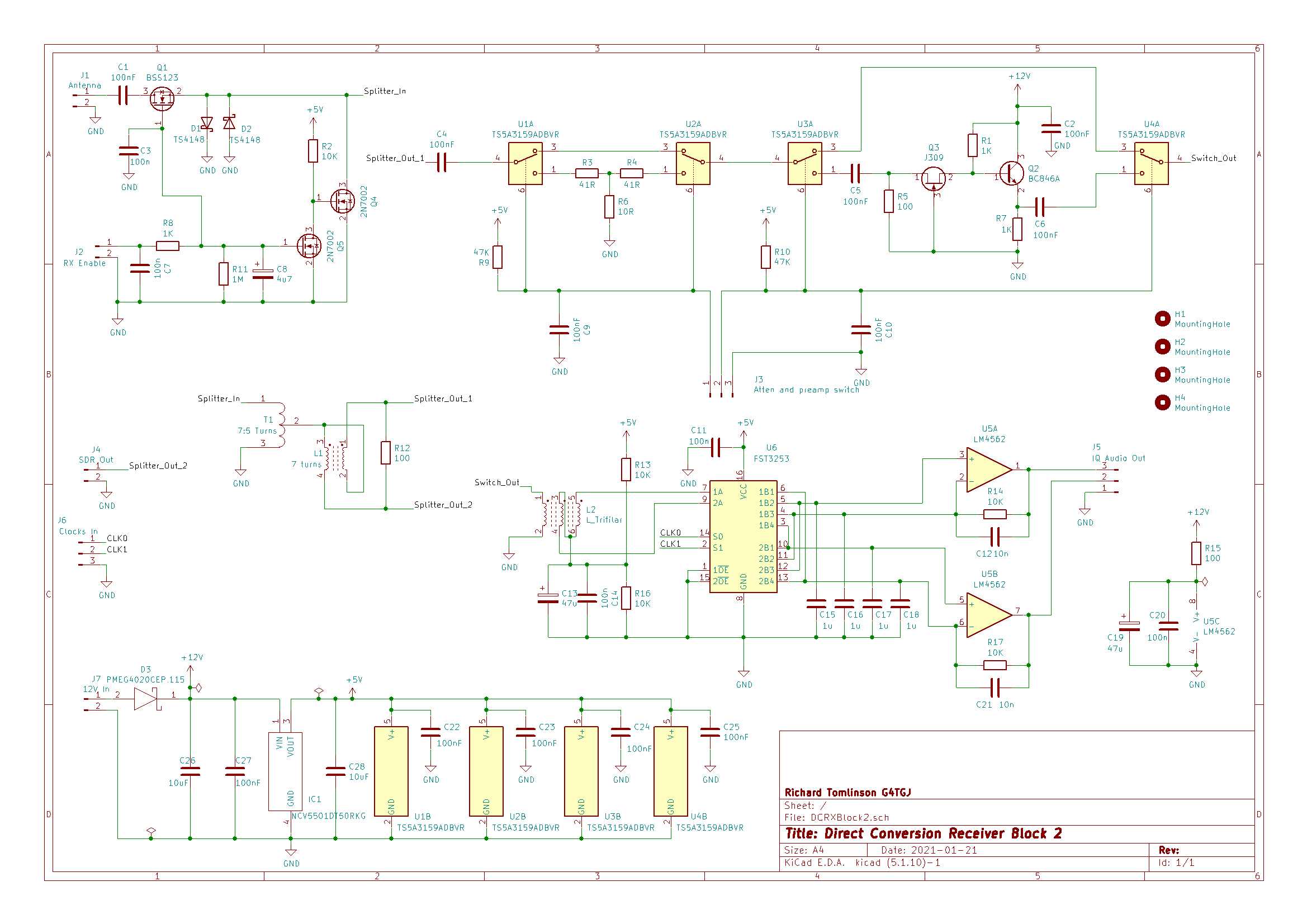
Q1, Q4 and Q5 form a switch to mute the receiver on transmit. The enable line from J2 is high on receive switching on Q1 and Q5. This switches off Q4. On transmit the enable line is low switching off Q1 and Q5. This causes Q4 to be switched on by R2 shorting out the receiver input. When switching between transmit and receive C8 charges or discharges through R8 so that the transition is not too abrupt. R11 is there to ensure the the gates of Q1 and Q5 are grounded if there is no connection to the enable line.
D1 and D2 offer additional protection from transmit signals. Q1 needs to withstand high transmit voltages. I used a BSS123 as I managed to blow a 2N7002 on transmit here. Q4 and Q5 could also be BSS123 (or probably almost any small MOSFET) as could all the other MOSFETs in the transceiver, except for the transmit PAs.
T1, L1 and R12 form a splitter with one output on J4. This connects to a BNC socket for feeding to an SDR receiver for use as a panadapter. The circuit is designed to keep a constant 50R impedance.
Analogue switches U1 and U2 switch the 20dB attenuator R3, R4 and R6 in and out of circuit. U3 and U4 switch the preamp formed by Q2 and Q3 in and out. The switches are normally on by R9 and R10 but can be switched off by grounding pin 1 or 2 on J3. This is done through two front panel switches.
L2 (6 turns trifilar on T50-43) provides differential signals for U6, the FST3253 Tayloe detector, with differential outputs connected to U5 which provides around 30dB of gain before feeding the I and Q signals to J5. The two quadrature clocks from the clock and control board are fed to J6.
J7 is the 12V input with D3 protecting against reverse polarity and IC1 is a 5V regulator for the FST3253.
Next article - Phasing audio filter and amplifier board