5 Band CW QRP Transceiver Phasing Audio Filter and Amplifier Board
Part of the 5 band transceiver.
The phasing audio filter and amplifier board is the final board required to build the receiver. It takes the in-phase (I) and quadrature (Q) audio from the direct conversion receiver
block and applies a 90 degree phase shift to cancel the image, sends it through a 200Hz CW filter and amplifies it for headphones.
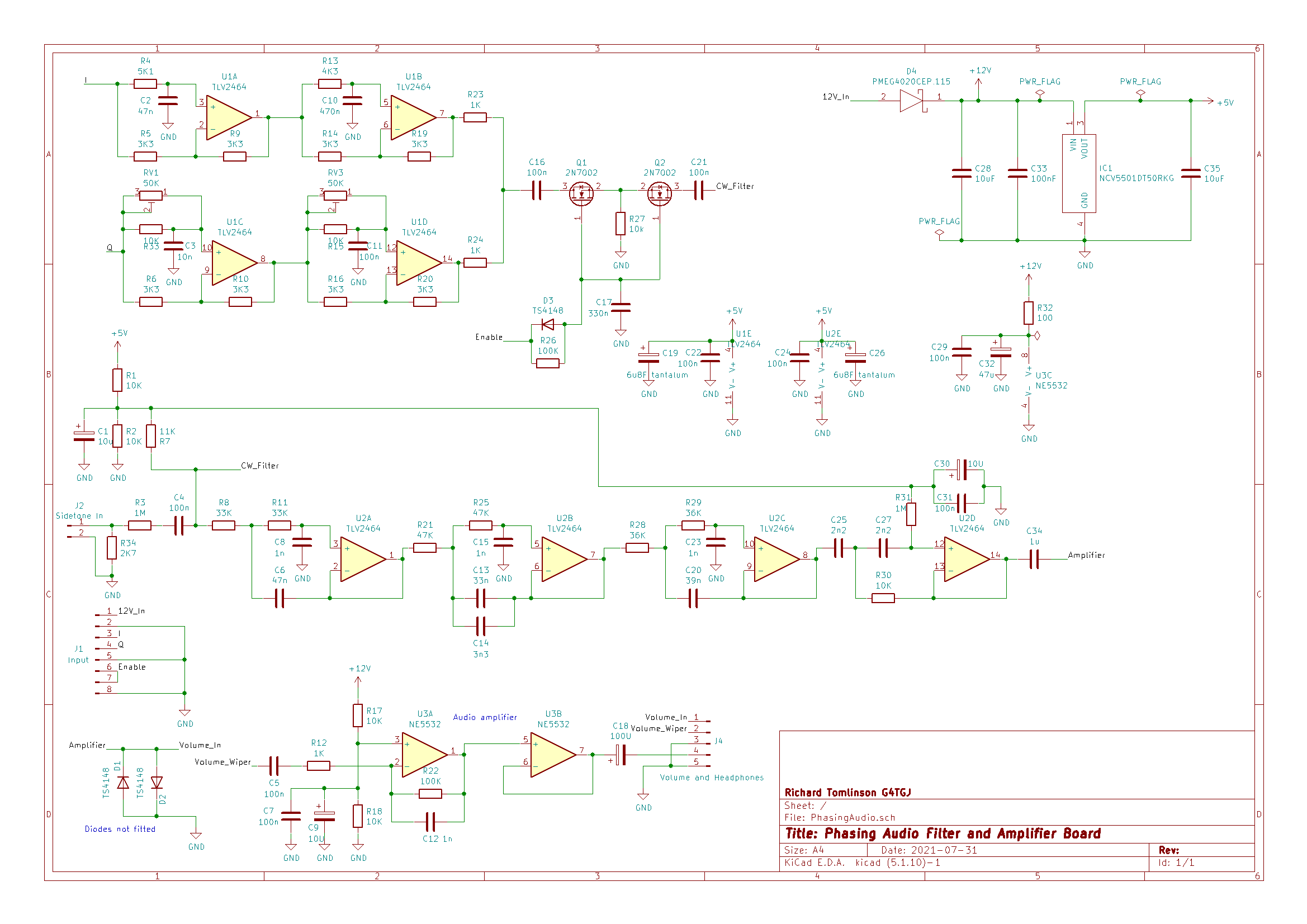
U1 forms a pair of all-pass filters that result in a 90 degree phase shift between I and Q. These are combined through R23 and R24. The phase shift is adjusted with RV1 and RV3 so that the wanted signal is strong and the unwanted image is inaudible.
Q1 and Q2 form a mute switch. Although there is a switch in the front end to isolate the receiver during transmit there are still clicks that make it through to the audio so there is another switch here in the audio path. The two MOSFETs are back-to-back so that the body diodes do not allow the clicks to get through. The switch is controlled by the same enable line as the front end switch. On transmit, enable goes low and D3 ensures the two transistors are turned off immediately and C17 is discharged. On return to receive the enable line goes high and C17 slowly charges through R26 so there is a slight delay before the receiver is fully active. Again, this is to prevent clicks getting through. The MOSFETs switch on when there is sufficient voltage between gate and source. R27 is required so that the source (or drain on one of the transistors) is at ground potential - 10K is high enough not to affect the audio.
U2 forms a 200Hz CW filter with R1 and R2 creating a virtual ground. Sidetone is generated by the microcontroller and fed in from J2 via the 1M resistor R3. The CW filter helps turn the square wave into a nice tone.
U3A is an audio amplifier with 40dB of gain. Again it has a virtual ground formed by R17 and R18. Note that this op-amp runs from 12V whereas the others are 5V. U3B is a buffer to drive the headphones.
J4 has connections for a 10K log pot for the volume control and to go to the headphone socket. Diodes D1 and D2 were intended to attenuate very loud signals but I found they distorted the audio so I removed them. If the signals are loud I just have to quickly turn the volume down!
J1 has the 12V DC and I/Q audio inputs. It also has the enable signal input with an output to daisy chain to the DC receiver block. The 12V input connects to D4 to protect against reverse polarity and IC1 is a 5V regulator for the op-amps.
All the capacitors in the audio chain need to be of good quality. The cheaper class 2 ceramics, such as X7R, can be microphonic and their value is affected by any voltage across them. I used NP0/C0G ceramics where available (and not too expensive) and film capacitors otherwise. If you were to build this with through-hole components then you might use Mylar throughout but with surface mount the film capacitors have a tendency to melt if you are not very careful with the soldering iron, hence the preference for class 1 ceramics. I laid out the board for 1210 size capacitors which is also compatible with 1206.
Much of this circuitry was inspired by the QCX, in particular the phasing filter U1 and the CW filter U2. The latter originally came from the Hipermite and the phasing filter was described by Dan Tayloe in the Norcal NC2030 back in 2005, so it’s not new.
Next article - Transmit board