5 Band CW QRP Transceiver Transmit Board
Part of the 5 band transceiver.
The final board for the transceiver is the transmit board. Actually there are 5 boards, one per band. You can, of course, build fewer boards for whichever bands interest you. The limitation of 5
is due to the number of I/O lines that are available on the the microcontroller. More could be supported by using an external I/O chip or decoder.
This would require software changes, although they would be straightforward.
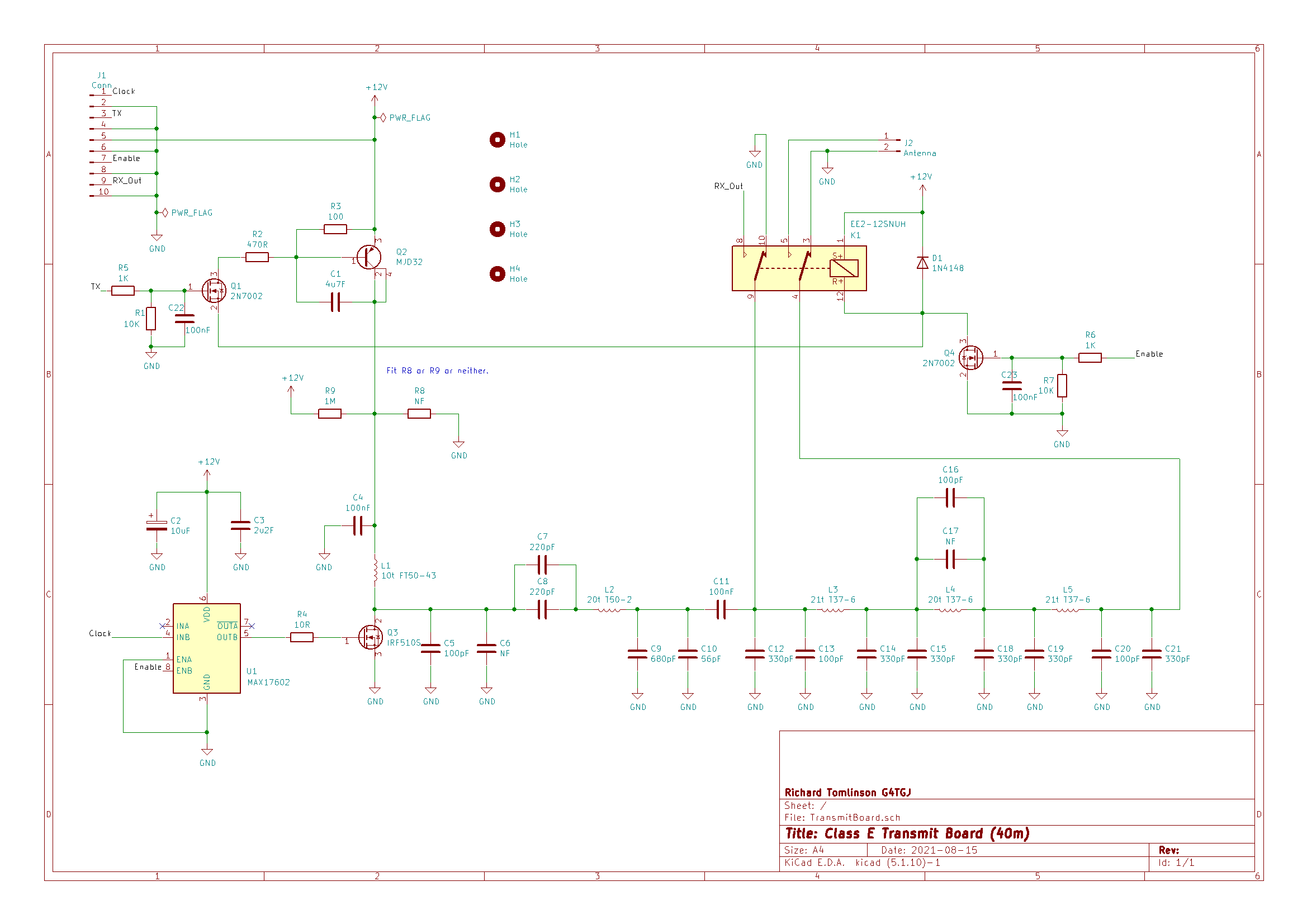
J1 is the main connector taking 12V DC in, clock, TX and enable lines from the clock and controller board and the RX output which connects to the antenna input on the receiver block board. Except for the enable line, these connections are all in parallel between all the transmit boards. I had originally intended building a backplane board which each transmit board would plug in to but in the end I connected all the boards using pin header leads. For the higher frequency bands (30m and 20m) I did make direct solder connections as I found the pin headers don’t work so well at these frequencies.
The enable line selects the band in use. If the band is enabled then Q4 energises the relay which connects the antenna to the output of the low pass filter and connects the other end of the filter to the receiver. Q4 also grounds the source of Q1 which is connected to the transmit line. Since all boards share the TX signal this ensure that only the active band board transmits. On transmit Q1 grounds the gate of Q2, a PNP power transistor, to provide 12V to the MOSFET PA. R2, R3 and C1 form a Miller integrator to provide some key shaping to the signal. This ensures that the output rises and falls slowly on key down and up to prevent key clicks.
The clock signal is fed to U1 which is a dual MOSFET driver. We are not using the A side so its enable line is grounded. The B side is non-inverting and is enabled by the band enable line. Q3 is the class E power amplifier driven via R4 which is to prevent parasitic oscillations. The transistor is the IRF510S which is the surface mount version of this familiar MOSFET. The drain is connected to a reasonable size area on the PCB to form a heatsink. I have never noticed them get warm. L1 is an RFC choke to provide a drain load. The class E network is formed by C5-C10 and L2. The values in the schematic are for the 40m band - see the table for the other bands. You may to need to change the turns on L2, or at least their spacing. Removing turns will increase the power output. You should be able to get 5W output. C12-21 and L3-L5 are the low pass filter to remove harmonics and provide some filtering on receive. Again the values are for 40m. The values are published by the G-QRP Club. The capacitors for the class E network and the LPF should be quality NP0/C0G types.
J2 is the antenna connector and is wired to the back panel BNC socket. I found it best to solder the wire to the PCB rather than using a pin header, especially on the higher bands. It’s also a good idea to make sure all the boards’ ground are well bonded together with additional wires or even braid from coax. I also stack the boards with brass stand-offs and this is another earth connection. Poor grounding is noticeable on receive.
R8 and R9 were late additions. I found some strange effects, initially only obvious when using the preamp on 30m. I found that immediately after transmitting, the receiver would be louder and then it would gradually get quieter. I spent ages trying to work out if the preamp was being triggered to oscillate by the transmitter. But I then realised that it was happening on 20m and 30m with or without the preamp. I eventually found that there was a voltage on the drain of the PA which gradually increased after transmit due to leakage in Q2. The charge on the MOSFET was probably affecting the drain to source capacitance which was attenuating the received signal. On transmit the PA uses up all this charge and so the received signal is louder. The solution was to fit the 1M resistor R8 from the drain circuit to ground so that the charge never builds up. I also noticed that the 40m band had the opposite problem where, immediately after transmit, the receiver was less sensitive. The solution here was to fit 1M resistor R9 from the drain circuit to 12V. I also did this for 60m but 80m does not appear to suffer either problem so the resistors are not needed. This may be because the band noise is much greater on 80m.
| Component | 80m | 60m | 40m | 30m | 20m |
|---|---|---|---|---|---|
| C5 | 470pF | 270pF | 100pF | 150pF | 47pF |
| C6 | NF | NF | NF | NF | NF |
| C7 | 470pF | 560pF | 220pF | 330pF | 220pF |
| C8 | 390pF | 30pF | 220pF | NF | NF |
| C9 | 1200pF | 1000pF | 680pF | 470pF | 330pF |
| C10 | 270pF | NF | 56pF | 47pF | 47pF |
| C12 | 470pF | 560pF | 330pF | 150pF | 220pF |
| C13 | 390pF | NF | 100pF | 150pF | NF |
| C14 | 1200pF | 470pF | 330pF | 470pF | 330pF |
| C15 | 100pF | 390pF | 330pF | NF | NF |
| C16 | 150pF | 120pF | 100pF | 68pF | 47pF |
| C17 | 47pF | NF | NF | NF | NF |
| C18 | 1200pF | 470pF | 330pF | 470pF | 330pF |
| C19 | 100pF | 390pF | 330pF | NF | NF |
| C20 | 470pF | 560pF | 330pF | 150pF | 220pF |
| C21 | 390pF | NF | 100pF | 150pF | NF |
| L2 | 28t T50-2 | 23t T50-2 | 20t T50-2 | 18t T50-6 | 14t T50-6 |
| L3 | 26t T37-2 | 24t T37-6 | 21t T37-6 | 18t T37-6 | 15t T37-6 |
| L4 | 25t T37-2 | 23t T37-6 | 20t T37-6 | 17t T37-6 | 14t T37-6 |
| L5 | 26t T37-2 | 24t T37-6 | 21t T37-6 | 18t T37-6 | 15t T37-6 |
| R8 | NF | NF | NF | 1M | 1M |
| R9 | NF | 1M | 1M | NF | NF |
NF = No Fit
When constructing the boards I started with the MOSFET driver U1 and all the transistors except the PA transistor Q3. I checked that the enable line, transmit signal and clock worked OK. I then build the LPF and wired in two temporary SMA sockets so that I could check the filter response on my nanoVNA. Once happy with this I added Q3 and its class E network, connected to a dummy load and powered the board via an ammeter. On transmit I could check for 5W output, making adjustments to L2 as required. Another way to increase the output is to lower C5/C6 but if you try this I suggest you monitor the PA drain voltage with an oscilloscope. If the capacitor is too small the drain voltage can get too high. It ought to be around 50-60V so that it is well within the IRF510S’s 100V limit for Vds (an antenna mismatch could make the drain voltage much higher). Once I was happy the PA was working I added the relay and its diode and incorporated the board within the transceiver.
The total current draw while transmitting 5W should be around 700-850mA, with higher draw on the higher frequencies. On receive it’s about 120mA. I estimated the MOSFET driver takes about 100mA and the drain voltage is about 13.3V (with a 13.8V supply). So the PA efficiency is about 60-80% depending on the band. Class E is often quoted as being better than this but the IRF510S has a fair amount of capacitance which is why it is less efficient at the higher frequencies. It might be possible to play with the network values more but I am happy with the output from these cheap devices.
I used ClassE from Tonne Software to design the Class E network and L match to 50 ohm and then spent some time optimising the values to get about 5W with reasonable efficiency.
Next article - User guide